

- Home
- Department
- Research
- Teaching
- Post Graduate Studies
- Knowledge Transfer
- How To


Electronic and Structural Properties of Thin Films
Research Strand:
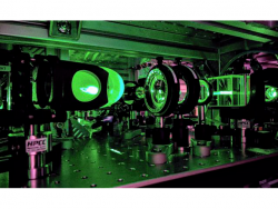
 The research activity is mainly carried out by means of experimental techniques based on the use of synchrotron radiation and in particular of the synchrotron beamline ALOISA at Elettra, the third-generation source of synchrotron radiation located in Trieste. This beamline, of which I am scientific and operational manager, has been available to external users since March 1998, and enables researchers to investigate the structural and electronic properties of thin films and crystal surfaces with a variety of experimental techniques such as X-ray absorption and photoemission spectroscopies (NEXAFS, HRXPS, valence Bband photoemission, photo-electron diffraction and grazing incidence X-ray diffraction (GIXD). It also features a system for in situ growth of thin layers using a molecular beam epitaxy technique. The monochromator, which covers an extremely wide range of photon energies (150 to 8000 eV), is unmatched in the world.
The combination of these techniques available on ALOISA is ideal for the study of thin films of organic materials, and this is the area our research group has been concentrating on. Of particular siginificance are the possible technological applications for the production of photovoltaic energy, since the use of organic materials for photovoltaic cells would make them much cheaper than the present ones based on crystalline or polycrystalline silicon, thereby rendering solar energy competitive with fossil fuels also from the point of view of production costs for industry.
More recently, we have been focusing in particular on the study of charge transfer processes at organic-organic and organic-inorganic interfaces. To this aim, we have made extensive use of the resonant photoemission (RESPES) technique for the study of charge-transfer phenomena which occur at the femtosecond time-scale, which are important to understand the properties of the organic materials relevant for photovoltaics. In fact, very often the efficiency of the charge transfer processes at interfaces is the limiting factor for overall cell efficiency. RESPES measurements are carried out in conjunction with single molecule conductivity measurements using the "break junction" method, an innovative technique that enables us study the quantum charge transport in the single molecule.
Also as part of the study of thin films, in collaboration with research groups at Columbia University we have used photoelectron microscopy techniques and electron microscopy (PEEM, XPEEM, MicroARUPS) to study the electronic properties and morphology of graphene layers obtained by mechanical exfoliation and deposited on Si / SIO or suspended on micro-holes. The measurements have shown for the first time the role played by corrugation, also present in the suspended graphene, in the electronic properties of this material. These results are of great importance for understanding the mechanisms of charge transport in graphene.
Recently we applied a combination of the techniques of He atom scattering (HAS) and synchrotron radiation spectroscopy to the study of nanostructures formed by molecules of biological interest (amino acids) on metal surfaces, in collaboration with research groups at the University of British Columbia, Vancouver and the Technical University of Monaco.
Info
Last update: 04-08-2024 - 20:50